Miniaturization Trends in PCB Assembly
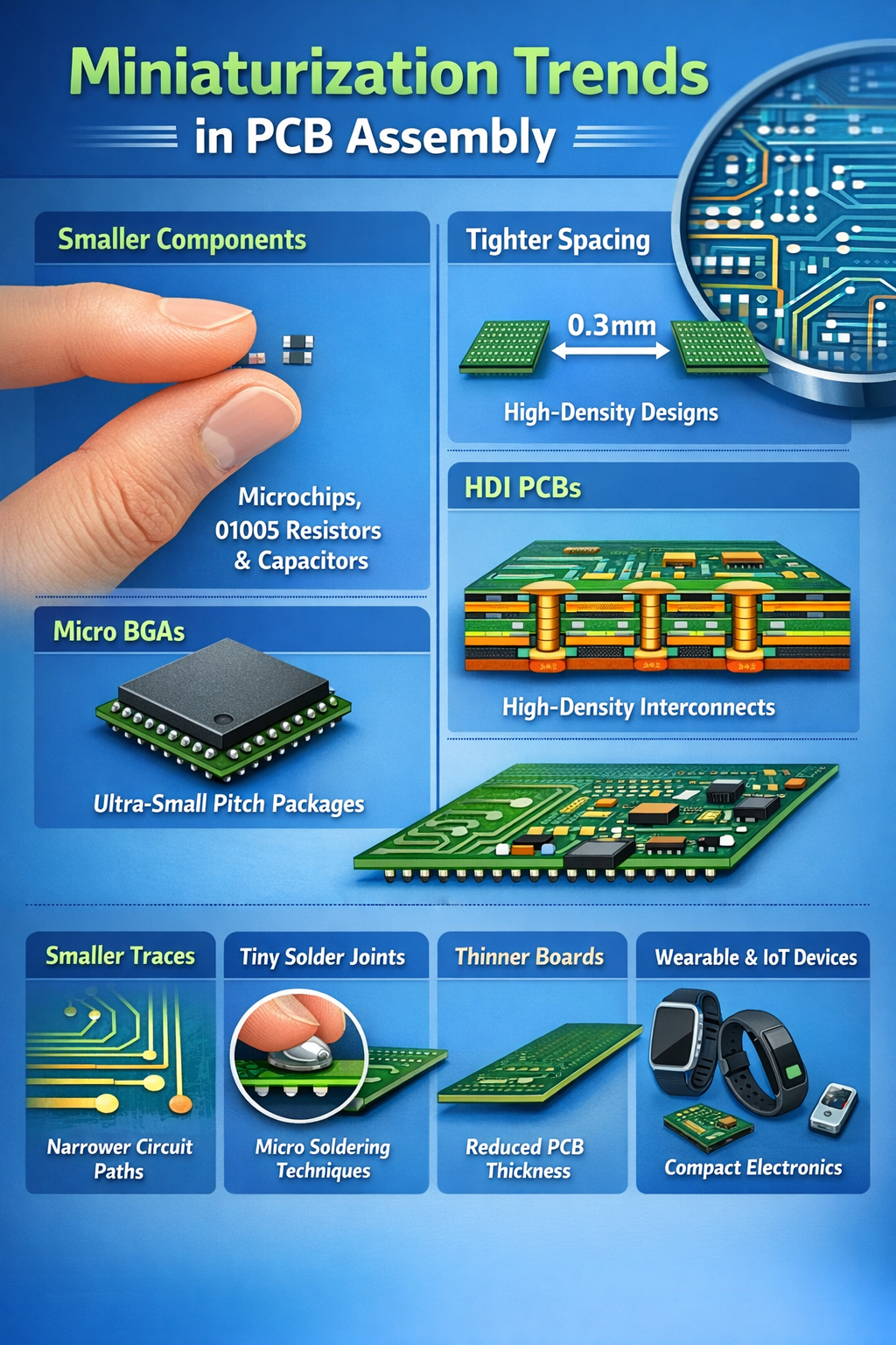
Electronic products are becoming smaller, lighter, and more powerful. From wearable devices and IoT modules to automotive control units and compact consumer electronics, the demand for reduced form factors continues to reshape manufacturing standards.Miniaturization is no longer just a design preference, it is a competitive requirement.
However, shrinking board size while increasing functionality introduces significant complexity in PCB assembly. Advanced PCB assembly services play a critical role in enabling manufacturers to achieve compact designs without compromising reliability.
Why Miniaturization Is Accelerating
Several industry forces are driving smaller PCB designs:
- Consumer demand for compact and portable devices
- Higher functionality within limited space
- Integration of wireless connectivity modules
- Battery-powered product ecosystems
- Consolidation of electronic control systems
As devices integrate more processing power, sensors, and communication modules into reduced footprints, PCB layout density increases significantly. PCB Assembly Services must adapt their processes to handle tighter tolerances and higher component density.
High-Density Interconnect (HDI) Adoption
One of the defining trends in miniaturization is the rise of High-Density Interconnect (HDI) PCBs.
HDI boards typically feature:
- Microvias
- Blind and buried vias
- Finer trace widths
- Higher layer counts
- Compact BGA footprints
These structures allow more routing within a smaller area. However, they require precise fabrication control and advanced PCB Assembly Services capable of managing fine geometries and strict process parameters.
Fine-Pitch and Micro Components
Miniaturized designs increasingly use:
- 0201 and 01005 passive components
- Fine-pitch QFN and BGA packages
- Wafer-level chip scale packages (WLCSP)
Handling and placing such small components demands high-accuracy SMT equipment and tightly controlled solder paste printing. Even slight variations in paste volume can lead to defects such as tombstoning or insufficient solder joints.
Professional PCB Assembly Services integrate precision placement systems and solder paste inspection (SPI) to maintain process stability.
Multi-Layer Boards and Stack-Up Optimization
As board area decreases, vertical expansion through multi-layer stack-ups becomes necessary.Advanced stack-up designs help:
- Maintain signal integrity
- Reduce electromagnetic interference
- Support high-speed communication
- Improve power distribution
However, increased layer count introduces thermal complexity during reflow. PCB Assembly Services must carefully control thermal profiling to ensure uniform heat distribution across dense board structures.
Thermal Management in Compact Designs
Miniaturized boards often house high-performance processors and power components in limited space, leading to localized heat concentration.Effective PCB Assembly Services collaborate with design teams to ensure:
- Thermal via placement under power devices
- Copper balancing strategies
- Optimized component spacing
- Controlled reflow parameters
Improper thermal management can reduce product lifespan and increase field failure rates.
Manufacturing Challenges Introduced by Miniaturization
Miniaturization increases process sensitivity across the assembly line.
1. Reduced Process Margins
Smaller components leave minimal tolerance for placement and soldering errors.
2. Inspection Complexity
Detecting defects in micro BGAs and fine-pitch components often requires AOI and X-ray inspection systems.
3. Board Warpage
Thin, high-layer-count boards are more susceptible to warping during thermal cycles.
4. Moisture Sensitivity
Smaller packages may have higher moisture sensitivity, increasing the importance of controlled storage and baking procedures.Reliable PCB Assembly Services implement strict environmental control and process monitoring to mitigate these risks.
Automation and Precision Equipment
To support miniaturization, advanced PCB Assembly Services invest in:
- High-speed, high-accuracy pick-and-place systems
- Laser-cut stencils for precise solder paste deposition
- Closed-loop inspection systems
- Multi-zone reflow ovens with controlled thermal gradients
- Data-driven Statistical Process Control (SPC)
Automation ensures consistency even at extremely fine tolerances.
Industry Applications Driving Miniaturization
Consumer Electronics
Wearables and portable devices demand ultra-compact PCBs with integrated functionality.
Automotive Electronics
Control modules are shrinking while integrating advanced features.
IoT Devices
Edge computing modules require compact layouts without compromising connectivity performance. In each of these industries, PCB Assembly Services must balance density with durability.
Reliability Considerations
Miniaturization increases electrical and mechanical stress concentration. Therefore, maintaining reliability requires:
- Controlled reflow profiling
- Accurate solder joint geometry
- Thermal cycling validation
- Vibration resistance testing
- Signal integrity analysis
PCB Assembly Services that integrate DFM review, process validation, and inspection control are better positioned to manage these reliability demands.
Conclusion
Miniaturization trends in PCB assembly are reshaping the electronics manufacturing landscape. Higher component density, finer pitches, and complex multi-layer structures demand precision engineering and strict process discipline.
Professional PCB Assembly Services enable manufacturers to achieve compact, high-performance designs while maintaining quality, scalability, and long-term reliability.
Miniaturization is not merely about reducing size, it is about delivering more capability in less space without sacrificing manufacturing stability or product performance.