PCB Assembly Techniques for Compact IoT Devices
The Internet of Things (IoT) has revolutionized the way devices communicate, collect data, and deliver functionality in real time. From wearable health monitors to industrial sensors and smart home products, IoT devices are becoming increasingly compact while delivering greater processing power.
This trend demands specialized PCB Assembly Services capable of meeting the unique challenges of miniaturization, high functionality, and low power consumption.
Challenges in IoT PCB Assembly
Designing and assembling PCBs for IoT devices is unlike traditional electronics manufacturing. Engineers must address:
- Limited Space: Compact IoT devices require maximum component density in minimal PCB real estate.
- Signal Integrity: High-speed communication and wireless modules demand precise routing and minimal interference.
- Power Efficiency: IoT devices often run on battery power, making low-power circuit design essential.
- Durability: Devices may be exposed to harsh environments, requiring reliable solder joints and protective coatings.
Key PCB Assembly Techniques for Compact IoT Devices
1. High-Density Interconnect (HDI) Technology
HDI PCBs use microvias, fine lines, and thinner materials to accommodate more components within a smaller footprint. This technique is essential for multi-function IoT devices like smartwatches or portable health trackers.
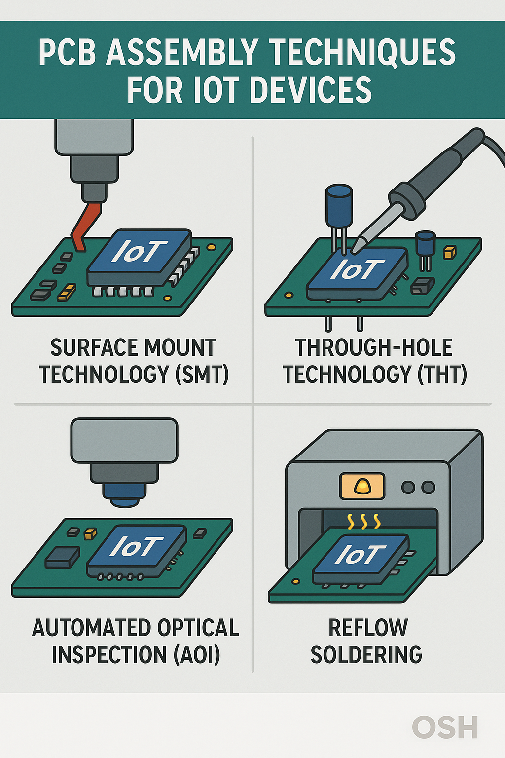
2. Surface Mount Technology (SMT) with Miniature Components
SMT enables the placement of extremely small components, such as 01005 or 0201 packages, directly onto the PCB surface. This method is ideal for increasing functionality without increasing device size.
3. Rigid-Flex PCB Designs
Combining rigid and flexible sections in a single PCB allows IoT devices to fit into unique form factors while maintaining electrical performance. This is common in wearables and foldable consumer gadgets.
4. Advanced Testing and Inspection
Compact IoT devices require precision testing such as automated optical inspection (AOI) and X-ray analysis to detect hidden solder defects in miniature components.
5. Conformal Coating for Environmental Protection
A thin protective layer shields the PCB from moisture, dust, and temperature variations, critical for IoT devices used in outdoor or industrial settings.
Why the Right PCB Assembly Partner Matters
Working with a specialized provider of PCB Assembly Services ensures that every stage, from component sourcing to final testing, is optimized for compact IoT designs.
The right partner understands the complexities of high-density layouts, low power requirements, and reliability standards unique to IoT applications.
Mefron Technologies: Precision for the IoT Era
Mefron Technologies delivers advanced PCB assembly solutions designed for the challenges of modern IoT devices.
Our capabilities in HDI manufacturing, micro-component placement, and rigorous testing processes ensure that every IoT product meets performance, size, and reliability requirements.
Final Thoughts
The success of compact IoT devices depends on more than just innovative design — it relies on precision PCB assembly techniques tailored to the constraints and demands of the application.
By leveraging the right manufacturing technologies and expertise, brands can create IoT devices that are smaller, smarter, and more reliable than ever before.